In the Spotlight
By Sharmini Jayawardena
PART II
❇‘Sweet spot’ in sweet material for hydrogen storage
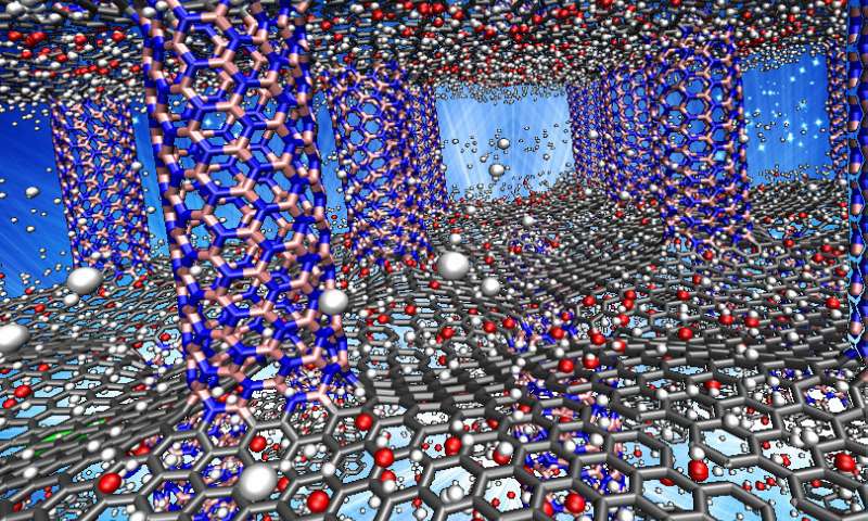
‘“The motivation is to create an efficient material that can take up and hold a lot of hydrogen – both by volume and weight – and that can quickly and easily release that hydrogen when it’s needed,” said the study’s lead author, Rouzbeh Shahsavari, assistant professor of civil and environmental engineering at Rice (University).’
‘The results appear in the journal Small.’
‘Hydrogen is the lightest and most abundant element in the universe, and its energy-to-mass ratio – the available energy per pound of raw material, for example – far exceeds that of fossil fuels. It’s also the cleanest way to generate electricity. The only byproduct is water. A 2017 report by market analysts at BCC Research found that global demand for hydrogen storage materials and technologies will likely reach $5.4 billion annually by 2021.’
‘Following months of calculations on two of Rice’s fastest supercomputers, Shahsavari and Rice graduate student Shuo Zhao found the optimal architecture for storing hydrogen in boron nitride. One form of the material, hexagonal boron nitride (hBN), consists of atom-thick sheets of boron and nitrogen and is sometimes called white graphene because the atoms are spaced exactly like carbon atoms in flat sheet of graphene.’
https://phys.org/news/2018-03-sweet-material-hydrogen-storage.html
https://phys.org/news/2018-03-method-large-single-crystal-graphene-advance.html
Method to grow large single-crystal graphene could advance scalable 2-D
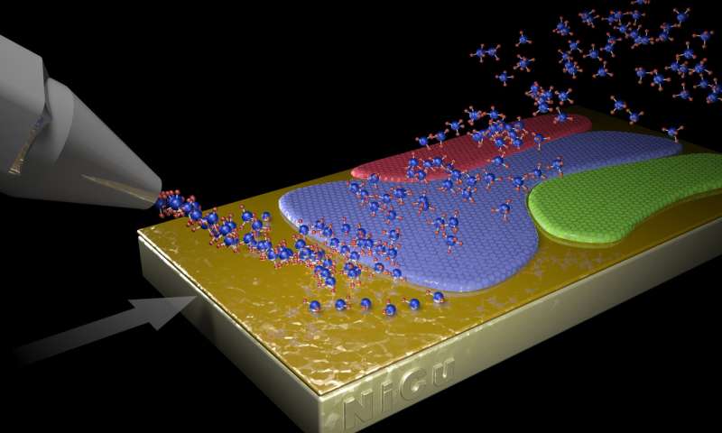
‘A new method to produce large, monolayer single-crystal-like graphene films more than a foot long relies on harnessing a “survival of the fittest” competition among crystals. The novel technique, developed by a team led by the Department of Energy’s Oak Ridge National Laboratory, may open new opportunities for growing the high-quality two-dimensional materials necessary for long-awaited practical applications.’
‘The team’s theoretician, led by coauthor Rice University professor Boris Yakobsen, provided a model…’
‘“If graphene or any 2-D material ever advances to industrial scale, this approach will be pivotal, similar to Czochralski’s method for silicon.”’
‘Yakobsen said, “manufacturers can rest assured that when a large, wafer-size raw layer is cut for any device fabrication, each resulting piece will be a quality mono-crystal…”’
‘Practical scaling up of graphene using the team’s method remains to be seen, but the researchers believe their evolutionary selection single-crystal growth method could be applied to promising alternative 2D materials such as boron nitride, also known as “white graphene,” molybdenum disulfide.
Ivan V Vlassiouk et al’
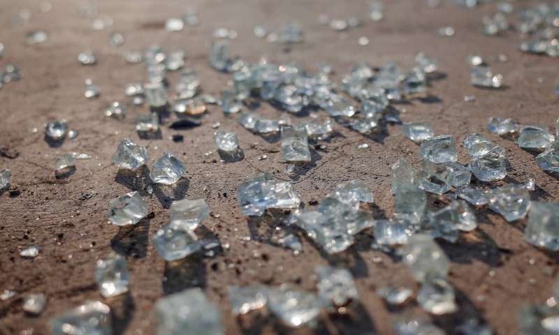
❇‘For millennia, people have used molten sand other ingredients to create glass and fashion beads, vessels, lenses and windows.
Liguid-to-glass transition process gains clarity
https://phys.org/news/2018-03-liquid-to-glass-transition-gains-clarity.html
‘In a liquid all of the atoms are moving past each other at all times. As a molten metal cools, and begins its transition to a solid, its atoms slow down and eventually stop moving.’
‘…a simple description might be that all of the atoms slow down together, at the same rate, until they stop moving and the material becomes a solid glass.’
“We have now demonstrated experimentally that is not what happens,” says Paul Voyles, material science and engineering professor at the University of Wisconsin-Madison.’
‘Now, he and his collaborators at Madison and Yale are working to understand how the atomic arrangements differ between the slow and fast parts.’
“That’s the next big missing piece of the puzzle,” he says.
‘The advance provides valuable information about the fundamental process through which every glass material – from window glass to plastic bottles to pharmaceutical preparations and many other – transition from liquid to solid, says Voyles.’
‘“…the ultimate potential impact of applications is if we really understand how this works at the atomic level, that gives us the opportunity to build in control that lets us make glasses out of what we want instead of only getting glasses when we get lucky.”’
❇‘Kagome Metal’: Physicists discover new quantum electronic material
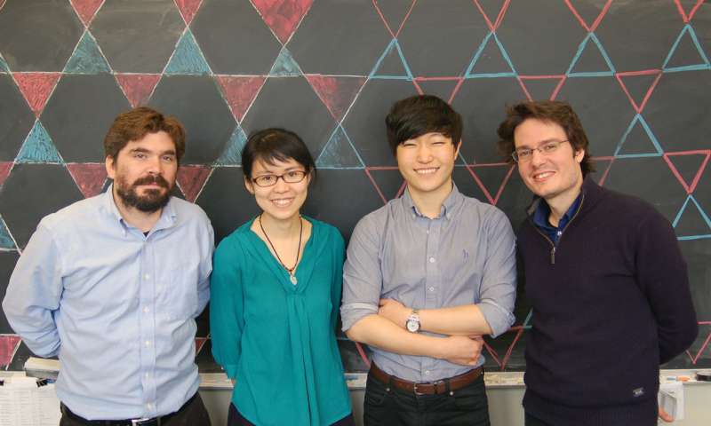
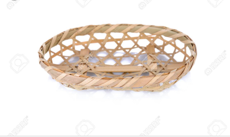
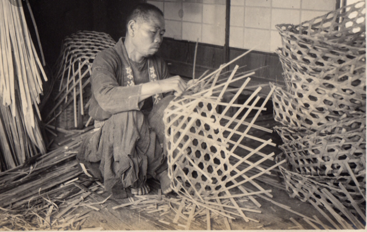
‘A motif of Japanese basket weaving known as the kagome pattern has preoccupied scientists for a long time.’
‘If a metal or other conductive material could be made to resemble such a kagome pattern at the atomic scale, with individual atoms arranged in similar triangular patterns, it should in theory exhibit exotic electronic properties.’
In a paper published 19 March 2018, in Nature, physicists from MIT, Harvard University, and Lawrence Berkeley National Laboratory report that they have for the first time produced a kagome metal – an electrically conducting crystal, made from layers of iron and tin atoms, with each atomic layer arranged in the repeating pattern of a kagome lattice.’
https://phys.org/news/2018-03-physicists-quantum-electronic-material.html
Kudos to all the wonderful scientists!
Kagome basket, basket weaving and leggings with kago.


![]()


