In the Spotlight
By Sharmini Jayawardena
There are materials, and materials, like Gypsum, prefabricated or precast concrete, pre-stressed concrete, reinforced concrete, plywood, MDF or medium density fiber board, chip board or particle board, PVC or polyvinyl chloride and others we have been all too familiar with over the past.
These are very basic materials that don’t lend themselves to much diversity in any way.
But, have you heard of the latest revolution taking place in the laboratories of the world

Graphene has taken the world of science
‘It has generated much excitement in the material-science research community due to its potential application in batteries, solar energy cells, touch screen and much more.’
Graphene goes beyond this area of applications. ‘Its unusual electron structure, under which its electrons behave like relativistic particles,’ is what the physicists are more interested in.
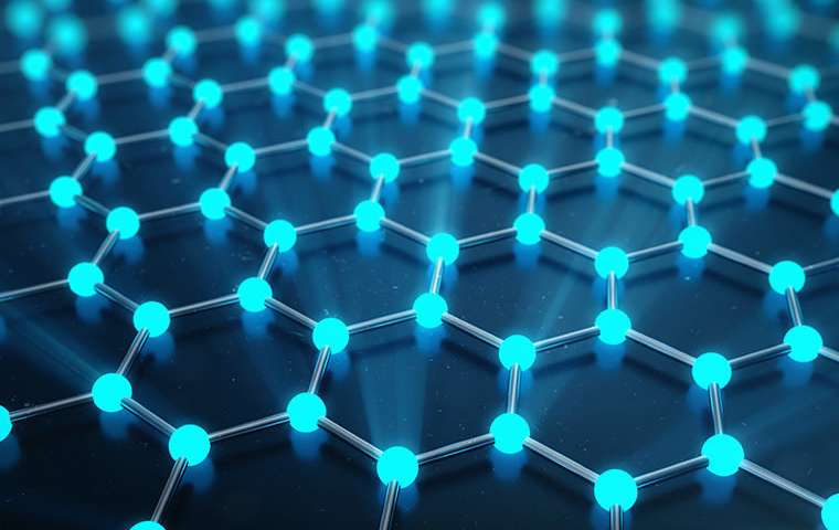
‘Electrons in graphene – an atomically thin, flexible and incredibly strong substance that captured the imagination of materials scientists and physicists alike – move at the speed of light, and behave like they have no mass…’
‘Deep in the sub-basement below Washington University’s historic Crow Hall, in St Louis, a research team led by Erik Henriksen, assistant professor of physics in Arts & Sciences, conducted its work in a custom-built vessel cooled to a few degrees above absolute zero.’
‘They use a small sliver of graphene sandwiched between two boron-nitride crystals and placed on top a silicon wafer; at approximately 16 microns long, the entire stack of material is less than one-sixth the size of a human hair.’
https://phys.org/news/2018-03-view-electron-interactions-graphene.html
The March Meeting of the American Physical Society is expected to bring together nearly 10,000 condensed-matter physicists, where other work by Henriksen’s lab will also be showcased. This will include a recent discovery that graphene can be used to measure a “quantum spin liquid” in magnetic materials.

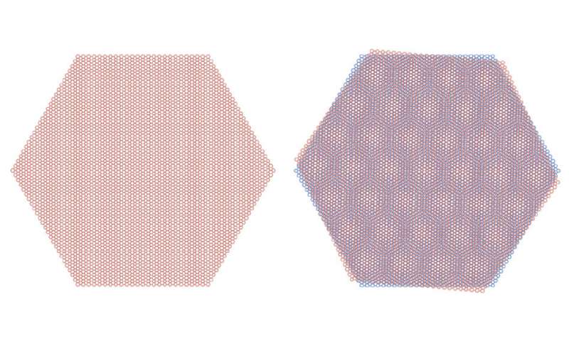
‘“Physicists at MIT and Harvard University have found that graphene, a lacy honeycomb-like sheet of carbon atoms, can behave at two electrical extremes – as an insulator, in which electrons are completely blocked from flowing; and as a superconductor, in which electrical current can stream through without resistance.”’ Nature
Credit: MIT
‘…essentially the most microscopic shaving of pencil lead you can imagine – is not just the thinnest material known in the world?, but also incredibly light and flexible, hundreds of times ?stronger than steel, and more 
‘“Usually, you have to grow different classes of materials to explore each phase,” says Jarillo-Herrero, “…we can explore all those physics in one device electrically, rather than having to make hundreds of devices. It couldn’t get any simpler.”’
https://phys.org/news/2018-03-rotated-magic-angle-graphene-sheets.html

Credit: Jiwoong Park et al
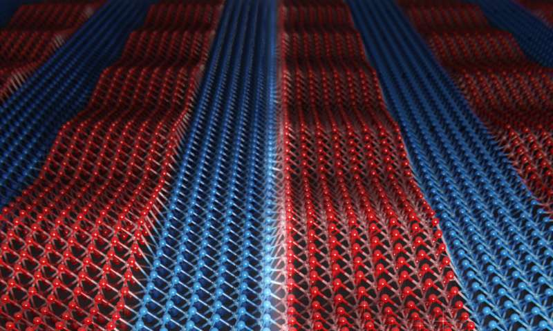
‘Joining different kinds of materials can lead to all kinds of breakthroughs. It’s an essential skill that allowed humans to make everything from skyscrapers (by reinforcing concrete with steel), to solar cells (by layering materials to herd electrons).’
‘In electronics, joining different materials, produces heterojunctions – the most fundamental components in solar cells (highlight), LEDs and computer chips. The smoother the seam between two materials, the more easily electrons flow across it, which is essential for how well electronic devices function…’
‘In a study published March 8, 2018, in Science, Cornell University and University of Chicago scientists revealed a technique to ‘sew’ two patches of crystals seamlessly together to create atomically thin fabrics.’
‘The resulting single-layer materials are the most perfectly aligned ever grown, according to the researchers. The gentler transition means that at the points where the two lattices meet, one lattice stretches or grows to meet the other – instead of leaving holes or other defects.”
‘“The new discovery opens up interesting ideas
https://phys.org/news/2018-03-atomic-lattices-seamlessly.html

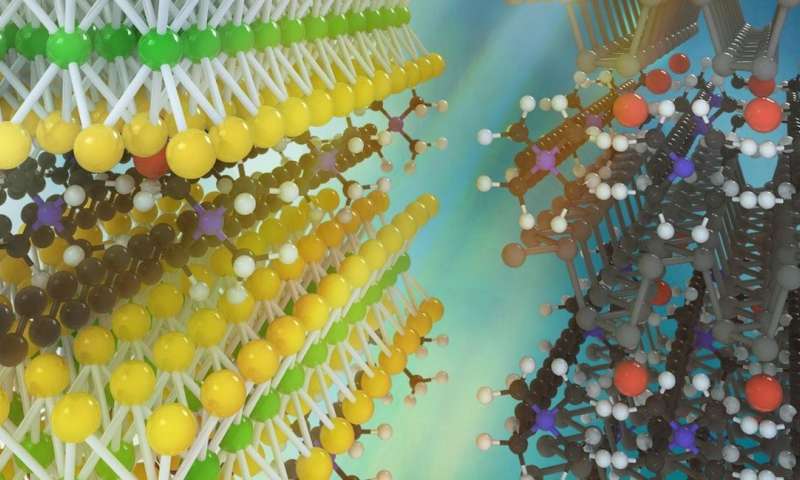
‘Artist’s concept of two kinds of monolayer atomic crystal molecular superlattices. On the left, molybdenum disulfide with layers of ammonium molecules, on the right, black phosphorus with layers of ammonium molecules.’
These new superlattices are called “monolayer atomic crystal molecular superlattices.”
‘The study? published in Nature, was led by Xiangfeng Duan, UCLA professor of chemistry and biochemistry, and Yu Huang, UCLA professor of materials science and engineering at the UCLA Samueli School of Engineering.’
https://phys.org/news/2018-03-class-two-dimensional-materials.html
‘“…The resulting materials could be useful in making faster transistors that consume less power, or for creating efficient light-emitting device,” Duan said.’
Chen Wang et al
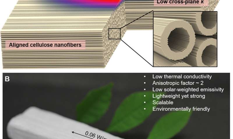
This is ‘nano wood,’ an invention that could reduce humanity’s carbon footprint
https://phys.org/news/2018-03-nanowood-humanity-carbon-footprint.html
“Completely derived from natural wood, nano wood with hierarchically aligned cellulose nanofibrils can be used as an anisotropic super thermal insulator. (A) Schematics of the thermally insulating properties of the nano wood. (B) Digital photograph of the nano wood and the corresponding properties beneficial for building insulation applications.”
Credit: Science and Advances (2018)
‘“Nature is producing this kind of material,” said senior author Liangbing Hu, a materials scientist?? and engineer at the University of Maryland in College Park.’
Keeping heat indoors during winter and keeping heat outdoors in the summer is a major issue in the cities. Managing heat in the cities we build with the current insulating materials we use are often very expensive to make, both monetarily and energy wise. They are also not biodegradable and ultimately contribute to our landfills.
‘“Hu has been probing the properties of nano-cellulose, nanometer-scale versions of cellulose, the tough carbohydrate in the cell walls of plants ? that allow tree?? trunks to grow strong and tall. At these incredibly small scales, cellulose fibers can take on remarkable characteristics, including a strength-to-weight ratio that’s about eight that of steel.”’
The secret of nano wood lies in its structure. While Styrofoam is isotopic, it basically looks the same from all angles, nano wood is anisotropic. The fibers of nano wood are bundled together in parallel, it looks very different from different angles. Heat can travel up and down the fibers with ease, but can’t cross them, because of the air gaps left after all the woody filler (lignin and hemicellulose) has been removed.
‘“Even better, nanocellulose is readily available and relatively cheap to process, costing as little as $7.44 per square meter…”’
‘“When the thickness is less than 1mm, the nano wood slice can be rolled and folded, making it suitable for scenarios that require flexibility, such as pipelines in chemical factories and power plants,” the author wrote.’
‘Hu said that such a strong, light weight, thermally insulating biodegradable material could have a host of future uses. It could be used to build skyscrapers, to manufacture cars
![]()


